Three-Dimensional Stacked Chip and Method for Manufacturing the Same
This overview is generated by Patentable from the patent's public abstract and description. The original USPTO text appears below.
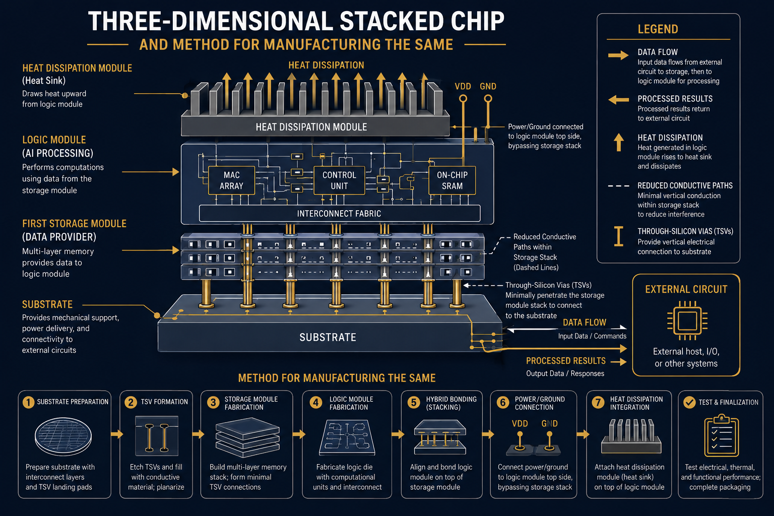
The present disclosure relates to a three-dimensional stacked chip and a method for manufacturing the same. The three-dimensional stacked chip includes a substrate, a first storage module, and a logic module. The first storage module and the logic module are sequentially stacked on the substrate, and the first storage module is arranged between the logic module and the substrate. The first storage module is configured to provide and store data required by the logic module, and support the logic module to complete corresponding work. The logic module is configured to perform signal exchange with the outside through the first storage module and the substrate. The disclosure can avoid impact of heat generated by the logic module on the storage module, significantly improve power consumption tolerance for the logic module and reduce the number of conductive paths in a storage module stacked structure effectively.
Legal claims defining the scope of protection, as filed with the USPTO.
the first storage module and the logic module are sequentially stacked on the substrate, and the first storage module is arranged between the logic module and the substrate; the first storage module is configured to provide and store data required by the logic module, and support the logic module to complete corresponding work; and the logic module is configured to perform signal exchange with the outside through the first storage module and the substrate. a substrate, a first storage module, and a logic module, wherein: . A three-dimensional stacked chip, comprising:
claim 1 the one or more stacked second storage modules are arranged between the first storage module and the logic module to form a storage module stacked structure with the first storage module; the one or more stacked second storage modules are configured to provide and store data required by the logic module, and support the logic module to complete corresponding work; and the logic module is configured to perform signal exchange with the outside through the storage module stacked structure and the substrate. one or more stacked second storage modules, wherein: . The three-dimensional stacked chip of, further comprising:
claim 2 the logic module is connected to a power supply by the storage module stacked structure, and is connected to the ground by a side opposite to the storage module stacked structure. . The three-dimensional stacked chip of, wherein:
claim 2 the logic module is connected to the ground by the storage module stacked structure, and is connected to a power supply by a side opposite to the storage module stacked structure. . The three-dimensional stacked chip of, wherein:
claim 2 the logic module comprises a plurality of stacked sub-logic modules; and the first storage module and the one or more stacked second storage modules are configured to provide and store data required by the plurality of stacked sub-logic modules, and support the plurality of stacked sub-logic modules to complete corresponding work. . The three-dimensional stacked chip of, wherein:
claim 5 a sub-logic module closer to the storage module stacked structure has lower power, and a sub-logic module farther away from the storage module stacked structure has higher power. . The three-dimensional stacked chip of, wherein:
claim 2 the first storage module is directly or indirectly arranged on the substrate, the one or more stacked second storage modules are directly or indirectly arranged on the first storage module as a whole, and the logic module is directly or indirectly arranged on the one or more stacked second storage modules. . The three-dimensional stacked chip of, wherein:
claim 2 the logic module is configured to obtain a work instruction from the external circuit through the substrate and the storage module stacked structure, complete corresponding work, and transmit a processing result through the storage module stacked structure and the substrate. . The three-dimensional stacked chip of, further comprising an external circuit arranged on the substrate, wherein:
claim 2 the Si interposer is arranged between the first storage module and the substrate, and the external circuit is arranged on the Si interposer; and the logic module is configured to obtain a work instruction from the external circuit through the Si interposer and the storage module stacked structure, complete corresponding work, and transmit a processing result through the storage module stacked structure and the Si interposer. . The three-dimensional stacked chip of, further comprising a silicon interposer (Si interposer) and an external circuit, wherein:
claim 2 the Si interposer is arranged between the first storage module and the substrate, and the external circuit is arranged on the Si interposer; and the logic module is configured to obtain a work instruction from the external circuit through the Si interposer, the substrate and the storage module stacked structure, complete corresponding work, and transmit a processing result through the storage module stacked structure, the Si interposer and the substrate. . The three-dimensional stacked chip of, further comprising a silicon interposer (Si interposer) and an external circuit, wherein:
claim 2 . The three-dimensional stacked chip of, further comprising a heat dissipation module arranged on the logic module directly or indirectly.
claim 11 . The three-dimensional stacked chip of, wherein the logic module is conductively connected to the heat dissipation module and is connected to a power supply or the ground by the heat dissipation module.
claim 12 . The three-dimensional stacked chip of, wherein the logic module is connected to the heat dissipation module by a conductive spacer layer.
forming a first stacked structure comprising a logic module and one or more second storage modules sequentially stacked on the logic structure; the second stacked structure comprises a first storage module, and the one or more second storage modules and a logic module sequentially stacked on the first storage module; the first storage module is obtained by processing the first storage structure; and the logic module is obtained by processing the logic structure; and forming a second stacked structure by using a first storage structure and the first stacked structure, wherein: connecting the first storage module to the substrate. . A method for manufacturing a three-dimensional stacked chip, comprising:
claim 14 the first storage structure comprises a first substrate, and a first storage device and a first interconnect layer formed on the first substrate; and the obtaining the first storage module by processing the first storage structure comprises: forming through-silicon vias (TSVs) running through the first substrate of the first storage structure. . The method for manufacturing a three-dimensional stacked chip of, wherein:
claim 14 the first storage structure comprises a first substrate, and a first storage device and a first interconnect layer formed on the first substrate; and thinning the first substrate of the first storage structure; and forming TSVs running through the thinned first substrate. the obtaining the first storage module by processing the first storage structure comprises: . The method for manufacturing a three-dimensional stacked chip of, wherein:
claim 14 the logic structure comprises a second substrate, and a logic device and a second interconnect layer formed on the second substrate; and thinning the second substrate of the logic structure; and forming TSVs running through the thinned second substrate. the obtaining the logic module by processing the logic structure comprises: . The method for manufacturing a three-dimensional stacked chip of, wherein
claim 14 . The method for manufacturing a three-dimensional stacked chip of, wherein the second storage module comprises a thinned third substrate, a second storage device and a third interconnect layer formed on the third substrate, and a fourth interconnect layer formed on a back of the thinned third substrate.
claim 14 . The method for manufacturing a three-dimensional stacked chip of, further comprising: arranging a heat dissipation module on the logic module.
claim 19 . The method for manufacturing a three-dimensional stacked chip of, wherein a conductive spacer layer and the heat dissipation module is sequentially arranged on the logic module, and the logic module is connected to the heat dissipation module through the conductive spacer layer to connect a power supply or the ground by the heat dissipation module.
Complete technical specification and implementation details from the patent document.
The present invention relates to the field of integrated circuit technologies, and more specifically, to a three-dimensional stacked chip and a method for manufacturing the same.
With the outburst of large language models in AI applications, artificial intelligence software has raised higher requirements on the chip design industry. A conventional chip architecture and supporting storage far cannot meet requirements of large language models for large bandwidths and high capacities. To meet the needs of explosive AI development, researches and development of novel chip architectures and new storage technologies need to be accelerated.
In view of the foregoing defects or improvement requirements of the related art, the present invention provides a three-dimensional stacked chip and a method for manufacturing the same, to avoid impact of heat generated by a logic module on a storage module, significantly improve power consumption tolerance for the logic module and reduce the number of conductive paths in a storage module stacked structure effectively.
To achieve the foregoing objective, according to one aspect of the present disclosure, the three-dimensional stacked chip includes a substrate, a first storage module, and a logic module. The first storage module and the logic module are sequentially stacked on the substrate, and the first storage module is arranged between the logic module and the substrate. The first storage module is configured to provide and store data required by the logic module, and support the logic module to complete corresponding work. The logic module is configured to perform signal exchange with the outside through the first storage module and the substrate.
In some implementations, the three-dimensional stacked chip further includes one or more stacked second storage modules, where the one or more stacked second storage modules are arranged between the first storage module and the logic module to form a storage module stacked structure with the first storage module; the one or more stacked second storage modules are configured to provide and store data required by the logic module, and support the logic module to complete corresponding work; and the logic module is configured to perform signal exchange with the outside through the storage module stacked structure and the substrate.
In some implementations, the logic module is connected to a power supply by the storage module stacked structure, and is connected to the ground by a side opposite to the storage module stacked structure.
In some implementations, the logic module is connected to the ground by the storage module stacked structure, and is connected to a power supply by a side opposite to the storage module stacked structure.
In some implementations, the logic module includes a plurality of stacked sub-logic modules; and the first storage module and the one or more stacked second storage modules are configured to provide and store data required by the plurality of stacked sub-logic modules, and support the plurality of stacked sub-logic modules to complete corresponding work.
In some implementations, a sub-logic module closer to the storage module stacked structure has lower power, and a sub-logic module farther away from the storage module stacked structure has higher power.
In some implementations, the first storage module is directly or indirectly arranged on the substrate, the one or more stacked second storage modules are directly or indirectly arranged on the first storage module as a whole, and the logic module is directly or indirectly arranged on the one or more stacked second storage modules.
In some implementations, the three-dimensional stacked chip further includes an external circuit arranged on the substrate, where the logic module is configured to obtain a work instruction from the external circuit through the substrate and the storage module stacked structure, complete corresponding work, and transmit a processing result through the storage module stacked structure and the substrate.
In some implementations, the three-dimensional stacked chip further includes a silicon interposer (Si interposer) and an external circuit, where the Si interposer is arranged between the first storage module and the substrate, and the external circuit is arranged on the Si interposer; and the logic module is configured to obtain a work instruction from the external circuit through the Si interposer and the storage module stacked structure, complete corresponding work, and transmit a processing result through the storage module stacked structure and the Si interposer.
In some implementations, the three-dimensional stacked chip further includes a silicon interposer (Si interposer) and an external circuit, wherein the Si interposer is arranged between the first storage module and the substrate, and the external circuit is arranged on the Si interposer; and the logic module is configured to obtain a work instruction from the external circuit through the Si interposer, the substrate and the storage module stacked structure, complete corresponding work, and transmit a processing result through the storage module stacked structure, the Si interposer and the substrate.
In some implementations, the three-dimensional stacked chip further includes a heat dissipation module arranged on the logic module directly or indirectly.
In some implementations, the logic module is conductively connected to the heat dissipation module and is connected to a power supply or the ground by the heat dissipation module.
In some implementations, the logic module is connected to the heat dissipation module by a conductive spacer layer.
forming a first stacked structure including a logic module and one or more second storage modules sequentially stacked on the logic structure; forming a second stacked structure by using a first storage structure and the first stacked structure, where the second stacked structure includes a first storage module, and the one or more second storage modules and a logic module sequentially stacked on the first storage module; the first storage module is obtained by processing the first storage structure; and the logic module is obtained by processing the logic structure; and connecting the first storage module to the substrate. According to another aspect of the present disclosure, a method for manufacturing a three-dimensional stacked chip is provided, including:
In some implementations, the first storage structure includes a first substrate, and a first storage device and a first interconnect layer formed on the first substrate; and the obtaining the first storage module by processing the first storage structure includes forming through-silicon vias (TSVs) running through the first substrate of the first storage structure.
In some implementations, the first storage structure includes a first substrate, and a first storage device and a first interconnect layer formed on the first substrate; and the obtaining the first storage module by processing the first storage structure includes thinning the first substrate of the first storage structure and forming TSVs running through the thinned first substrate.
In some implementations, the logic structure includes a second substrate, and a logic device and a second interconnect layer formed on the second substrate; and the obtaining the logic module by processing the logic structure includes thinning the second substrate of the logic structure and forming TSVs running through the thinned second substrate.
In some implementations, the second storage module includes a thinned third substrate, a second storage device and a third interconnect layer formed on the third substrate, and a fourth interconnect layer formed on a back of the thinned third substrate.
In some implementations, the method for manufacturing a three-dimensional stacked chip further includes arranging a heat dissipation module on the logic module.
In some implementations, a conductive spacer layer and the heat dissipation module is sequentially arranged on the logic module, and the logic module is connected to the heat dissipation module through the conductive spacer layer to connect a power supply or the ground by the heat dissipation module.
In general, compared with the related art, the foregoing technical solutions conceived in the present disclosure has the following beneficial effects: The storage module stacked structure is arranged between the logic module and the substrate, so that the logic module is arranged on the storage module stacked structure, thereby providing great convenience for heat dissipation of the logic module. The logic module is closer to the heat dissipation module than the storage module stacked structure, which avoids impact of heat generated by the logic module on the storage modules, and significantly improves power consumption tolerance for the logic module. In addition, the logic module is connected to a power supply or the ground by a side opposite to the storage module stacked structure without using the storage module stacked structure, thereby reducing the number of conductive paths (e.g., through-silicon vias) in the storage module stacked structure effectively.
To make the objectives, technical solutions, and advantages of the present invention clearer and more understandable, the present invention is further described below in detail with reference to accompanying drawings and embodiments. It should be understood that the specific embodiments described herein are used only for describing the present invention, and are not intended to limit the present invention. As a person skilled in the art can realize, the described embodiments may be modified in various different ways without departing from the spirit or the scope of this application. Therefore, the drawings and the description are to be considered as illustrative in nature but not restrictive.
1 FIG. Stacking a storage module and a logic module in a plurality of layers can multiply a bandwidth and a capacity of a system, so that requirements of a large language model can be fully met.shows a solution of a three-dimensional stacked chip.
1 FIG. 1 FIG. 103 105 101 105 103 103 105 101 103 103 103 105 105 105 103 103 As shown in, a logic moduleand a plurality of storage modulesare sequentially stacked on a substrate. The storage modulesare arranged on the logic module, and the logic moduleis arranged between the storage modulesand the substrate, which facilitates providing a proper power supply and the ground for the logic module, and facilitates data transfer between the logic moduleand the outside. In addition, the logic modulegenerates a large amount of heat when running, and the heat is mainly dissipated upward through a side on which the storage modulesare located. However, the storage modulesare very sensitive to heat, and the storage modulesstacked in a plurality of layers further limit heat dissipation. Particularly, when the logic moduleworks with high power consumption, such a stacking manner produces a serious heat accumulation effect, which greatly reduces power consumption tolerance for the logic module. Therefore, the three-dimensional stacked chip shown incannot meet requirements of a large language model on power consumption and computing power of a logic module.
1 FIG. To improve power consumption tolerance for the logic module and reduce adverse impact of heat accumulation on the storage modules, it is necessary to further improve the three-dimensional stacked chip shown in.
2 FIG. 201 203 207 205 203 207 205 201 203 207 205 201 205 As shown in, a three-dimensional stacked chip in this embodiment of the present invention includes a substrate, a first storage module, one or more second storage modules, and a logic module. The first storage module, the one or more second storage modules, and the logic moduleare sequentially stacked on the substrate. The first storage moduleand the one or more second storage modulesform a storage module stacked structure. The logic moduleis arranged on the storage module stacked structure. The storage module stacked structure is arranged between the substrateand the logic module.
203 207 203 201 205 207 207 207 207 207 207 207 207 207 One surface of the first storage moduleforms a conductive connection to an adjacent second storage module, and an other surface of the first storage moduleforms a conductive connection to the substrate. One surface of the logic moduleforms a conductive connection to an adjacent second storage module. When a second storage moduleis adjacent to another second storage moduleon one side, the surface of the second storage moduleon the side forms a conductive connection to the adjacent second storage module. When a second storage moduleis adjacent to another second storage moduleon both sides, the surfaces of the second storage moduleon both sides form conductive connections to the corresponding adjacent second storage modules.
205 203 207 205 203 207 203 207 205 205 203 207 205 Further, the logic moduleforms conductive connections to the first storage moduleand the one or more second storage modules, to enable the logic moduleto perform data exchange with the first storage moduleand the one or more second storage modules. Specifically, the first storage moduleand the one or more second storage modulesare mainly configured to provide and store data required by the logic module, and support the logic moduleto complete corresponding work. In some implementations, one or more of the first storage moduleand the one or more second storage modulescan further achieve a few logical control functions. To be specific, one or more of the storage modules are a combination of a storage medium and a logical medium. Such a combination may be a one-dimensional structure, or may be a two-dimensional structure or a three-dimensional structure. In some implementations, the function that can be implemented by the logic moduleincludes one or more of computing, control, interfacing, and data processing.
205 203 207 205 205 205 The logic moduleforms conductive connections to the first storage moduleand the one or more second storage modules, to form conductive paths in the storage module stacked structure, so that the logic modulecan perform signal exchange with the outside through the storage module stacked structure. In some implementations, the logic moduleis connected to a power supply by the storage module stacked structure, and is connected to the ground by a side opposite to the storage module stacked structure. In some implementations, the logic moduleis connected to the ground by the storage module stacked structure, and is connected to a power supply by a side opposite to the storage module stacked structure.
205 In some implementations, the logic moduleincludes a plurality of stacked sub-logic modules, and adjacent surfaces of the plurality of stacked sub-logic modules form a conductive connection. In some implementations, a sub-logic module closer to the storage module stacked structure has lower power, and a sub-logic module farther away from the storage module stacked structure has higher power, which helps dissipate heat of the sub-logic module with higher power, and reduces impact of heat on the storage module.
207 203 203 205 203 201 In some implementations, the one or more second storage modulesmay be omitted, to replace the storage module stacked structure with the first storage module. To be specific, one surface of the first storage moduleforms a conductive connection to the logic module, and an other surface of the first storage moduleforms a conductive connection to the substrate. The foregoing solution of arranging the logic module on the storage module is still applicable to a case in which there is only one storage module.
203 201 207 203 205 207 207 207 207 207 207 207 207 207 203 207 203 207 205 207 205 In some implementations, the foregoing manner of forming a conductive connection includes one or more of hybrid bonding and a conductive bump connection. In some implementations, the first storage modulemay be directly or indirectly arranged on the substrate, the one or more second storage modulesas a whole may also be directly or indirectly arranged on the first storage module, and the logic modulemay also be directly or indirectly arranged on the one or more second storage modules. In some implementations, being adjacent refers to being closest, and may be being directly adjacent or indirectly adjacent. For example, when there is no other second storage moduleor no other structure between two adjacent second storage modules, the two adjacent second storage modulesare directly adjacent. When there is no other second storage modulebetween two adjacent second storage modules, while another structure is further arranged between the two adjacent second storage modules, the two adjacent second storage modulesare indirectly adjacent. A second storage moduleadjacent to the first storage modulerefers to a second storage moduleclosest to the first storage module. A second storage moduleadjacent to the logic modulerefers to a second storage moduleclosest to the logic module.
201 203 201 201 205 201 205 201 201 In some implementations, an external circuit (for example, a GPU/CPU) is further arranged on the substrate. The external circuit forms a conductive connection to the first storage moduleby external interfaces and the substrate, and the substrateis connected to a circuit board (not shown in the figure) by external pins. In some implementations, the logic moduleis connected to the power supply and the ground by the storage module stacked structure and the substrate. Further, the logic moduleobtains a work instruction from the outside (the external circuit) through the substrateand the storage module stacked structure, completes corresponding work, and transmits a processing result (to the external circuit) through the storage module stacked structure and the substrate.
203 201 203 201 205 205 201 201 In some implementations, a silicon interposer (Si interposer) is arranged between the first storage moduleand the substrate. The Si interposer is used to provide a high-density electrical connection. An external circuit (for example, a GPU/CPU) is further arranged on the Si interposer. The external circuit forms a conductive connection to the first storage moduleby external interfaces and the Si interposer. The Si interposer further forms a conductive connection to external pins by external interfaces and the substrate, and is finally connected to a circuit board (not shown in the figure) by the external pins. In some implementations, the logic moduleis connected to the power supply and the ground by the storage module stacked structure and the Si interposer. Further, the logic moduleobtains a work instruction from the outside (the external circuit) through the Si interposer (or the Si interposer and the substrate) and the storage module stacked structure, completes corresponding work, and transmits a processing result (to the external circuit) through the storage module stacked structure and the Si interposer (or the Si interposer and the substrate).
201 203 207 In some implementations, the substrateis made of one or more of silicon, silicon germanium, germanium, silicon-on-insulator (SOI), and organic matter. In some implementations, the first storage moduleis a Flash, an RRAM, a DRAM, an MRAM, or an SRAM, and the second storage moduleis a Flash, an RRAM, a DRAM, an MRAM, or an SRAM.
2 FIG. 205 205 The structure shown inprovides convenience for the logic moduleto dissipate heat through the opposite side of the storage module stacked structure by placing the logic moduleon top of the storage module stacked structure, avoiding heat accumulation caused by the obstruction of heat conduction in both directions of the logic module when the logic module is between the storage module stacked structure and the substrate, and significantly reducing the impact of heat generated by the logic module on the storage module.
3 FIG. 301 205 301 205 301 205 205 301 205 301 205 301 301 205 301 205 301 As shown in, a heat dissipation moduleis arranged on the logic module. The heat dissipation modulecan ensure that a large amount of heat generated by the logic moduleduring high-power-consumption running is dissipated in time, so that power consumption tolerance for the logic module can be significantly increased. In some implementations, the heat dissipation modulemay be directly or indirectly arranged on the logic module. In general, a positional relationship among the storage module stacked structure, the logic module, and the heat dissipation moduleonly needs to satisfy that the logic modulewith high power is closer to the heat dissipation moduleat the top than the storage module stacked structure. In some implementations, the logic moduleforms a conductive connection to the heat dissipation moduleand is connected to a power supply or the ground by the heat dissipation module. In some implementations, the logic moduleis connected to the heat dissipation moduledirectly. In some implementations, the logic moduleis connected to the heat dissipation moduleby a conductive spacer layer.
4 FIG. 207 203 401 205 402 207 403 404 401 203 404 207 402 205 403 207 Further, as shown in, the three-dimensional stacked chip includes three second storage modules. The first storage moduleincludes a first substrate and a first interconnect layerarranged on a side of the first substrate. The logic moduleincludes a second substrate and a second interconnect layerarranged on a side of the second substrate. Each second storage moduleincludes a third substrate and a third interconnect layerand a fourth interconnect layerarranged on two sides of the third substrate. The first interconnect layerof the first storage moduleis bonded to a fourth interconnect layerof an adjacent second storage module, and the second interconnect layerof the logic moduleis bonded to a third interconnect layerof an adjacent second storage module.
207 207 403 207 404 207 401 207 403 207 207 207 403 207 404 207 404 207 403 207 When a second storage moduleis adjacent to another second storage moduleon one side, a third interconnect layerof the second storage moduleis bonded to a fourth interconnect layerof the adjacent another second storage module, or a fourth interconnect layerof the second storage moduleis bonded to a third interconnect layerof the adjacent another second storage module. When a second storage moduleis adjacent to another second storage moduleon both sides, a third interconnect layerof the second storage moduleis bonded to a fourth interconnect layerof the adjacent another second storage moduleon one side, and a fourth interconnect layerof the second storage moduleis bonded to a third interconnect layerof the adjacent another second storage moduleon the other side.
207 203 401 203 402 205 In some implementations, when the one or more second storage modulesare removed, and there is only the first storage module, the first interconnect layerof the first storage moduleis bonded to the second interconnect layerof the logic module.
401 402 403 404 In some implementations, the first interconnect layerincludes an insulation layer and conductive structures formed in the insulation layer. The second interconnect layerincludes an insulation layer and conductive structures formed in the insulation layer. The third interconnect layerincludes an insulation layer and conductive structures formed in the insulation layer. The fourth interconnect layerincludes an insulation layer and conductive structures formed in the insulation layer. In some implementations, bonding refers to chemical bonding of insulation layers of two interconnect layers, as well as physical interdiffusion of conductive structures of the two interconnect layers at an interface of the two interconnect layers, thereby forming a bonding interface between the interconnect layers.
203 405 207 407 205 409 The storage module stacked structure further includes a plurality of through silicon vias (TSVs). Specifically, the first storage moduleincludes a plurality of first TSVsrunning through the first substrate, each second storage moduleincludes a plurality of second TSVsrunning through the third substrate, and the logic moduleincludes a plurality of third TSVsrunning through the second substrate. In some implementations, forming the first TSVs includes forming hole structures running through the first substrate, and filling the hole structures with insulation material and conductive material. Forming the second TSVs includes forming hole structures running through the third substrate, and filling the hole structures with insulation material and conductive material. Forming the third TSVs includes forming hole structures running through the second substrate, and filling the hole structures with insulation material and conductive material.
205 203 207 205 203 207 205 205 Through conductive structures in the first to fourth interconnect layers and the first and second TSVs, the logic moduleforms conductive connections to the first storage moduleand the one or more second storage modules, and conductive paths are formed in the storage module stacked structure, which enables the logic moduleto exchange data with the first storage moduleand the one or more second storage modules, and exchange signals with the outside by the storage module stacked structure. In some implementations, the logic moduleconnects a power supply through conductive structures in the first to fourth interconnect layers and the first and second TSVs, and connects the ground through the third TSVs and the heat dissipation module. In some implementations, the logic moduleconnects the ground through conductive structures in the first to fourth interconnect layers and the first and second TSVs, and connects a power supply through the third TSVs and the heat dissipation module.
5 FIG.A 5 FIG.J 6 FIG. 5 FIG.A 5 FIG.C 600 toare schematic diagrams of a method for manufacturing a three-dimensional stacked chip according to an embodiment of the present invention.is a flowchart of an example methodfor manufacturing a three-dimensional stacked chip. First, with reference toto, a process of forming a first storage structure, a logic structure, and a second storage structure required for manufacturing a three-dimensional stacked chip is described.
5 FIG.A 501 503 503 505 507 505 503 503 A first storage structure is formed, including: forming a first storage device and a first interconnect layer on a first substrate. As shown in, a first storage device is formed on a first substrate, and then, a first interconnect layeris formed on the first storage device. The first interconnect layerincludes an insulation layerand a plurality of conductive structuresformed in the insulation layer. Apparently, a side on which the first interconnect layeris located is a face of the first storage structure, and a side opposite to the first interconnect layeris a back of the first storage structure. In some implementations, in addition to storage function, the first storage device can also achieve a few logical control functions. In some implementations, forming the first storage structure further includes forming conductive structures in the first substrate according to a predetermined thinning data of the first substrate.
5 FIG.B 509 511 511 513 515 513 511 511 A logic structure is formed, including: forming a logic device and a second interconnect layer on a second substrate. As shown in, a logic device is formed on a second substrate, and then, a second interconnect layeris formed on the logic device. The second interconnect layerincludes an insulation layerand a plurality of conductive structuresformed in the insulation layer. Apparently, a side on which the second interconnect layeris located is a face of the logic structure, and a side opposite to the second interconnect layeris a back of the logic structure. In some implementations, the function that can be implemented by the logic device includes one or more of computing, control, interfacing, and data processing. In some implementations, forming the logic structure further includes forming conductive structures in the second substrate according to a predetermined thinning data of the second substrate.
5 FIG.C 519 521 521 523 525 523 521 521 One or more (for example, three) second storage structures are formed in a manner similar to that of the first storage structure. Specifically, a second storage device and a third interconnect layer are formed on a third substrate, to form a second storage structure. As shown in, a second storage device is formed on a third substrate, and then, a third interconnect layeris formed on the second storage device. The third interconnect layerincludes an insulation layerand a plurality of conductive structuresformed in the insulation layer. Apparently, a side on which the third interconnect layeris located is a face of the second storage structure, and a side opposite to the third interconnect layeris a back of the second storage structure. In some implementations, in addition to storage function, one or more of the second storage device can also achieve a few logical control functions. In some implementations, forming the second storage structure further includes forming conductive structures in the third substrate according to a predetermined thinning data of the third substrate.
600 601 526 527 528 528 523 521 513 511 525 521 515 511 6 FIG. 5 FIG.D The example methodbegins with operation. As shown in, the second storage structure is inverted, the third interconnect layer is aligned with the second interconnect layer, and the second storage structure and the logic module are combined, to enable the second storage structure and the logic structure to form a conductive connection through the third interconnect layer and the second interconnect layer. As shown in, the second storage structureand the logic structureare combined in a face-to-face manner, to form a bonding interface. Specifically, forming the bonding interfaceincludes: enabling the insulation layerin the third interconnect layerand the insulation layerin the second interconnect layerto form chemical bonding at an interface, and enabling the conductive structuresin the third interconnect layerand the conductive structuresin the second interconnect layerto perform physical diffusion at the interface.
600 603 519 526 529 531 529 533 529 534 533 535 537 535 533 534 6 FIG. 5 FIG.E The example methodcontinues with operation. As shown in, the third substrate of the second storage structure is thinned, TSVs running through the thinned third substrate are formed, and a fourth interconnect layer is formed on the thinned third substrate to form a second storage module. As shown in, the third substrateof the second storage structureis thinned to obtain a thinned substrate, TSVsrunning through the substrateare formed, and a fourth interconnect layeris further formed on the substrate, to form a second storage module. The fourth interconnect layerincludes an insulation layerand a plurality of conductive structuresformed in the insulation layer. Apparently, a side on which the fourth interconnect layeris located is a back of the second storage module. In some implementations, by thinning the third substrate until conductive structures in the third substrate expose, the conductive structures forms TSVs running through the thinned third substrate.
In some implementations, the insulation layer in the first to fourth interconnect layers is one or more layers of insulation material, for example, silicon oxide, silicon nitride, silicon oxynitride, or a combination thereof. In some implementations, a process of forming conductive structures in the first to fourth interconnect layers includes: first forming openings in the insulation layer, and then filling required openings with conductive material. In some implementations, conductive material for manufacturing the conductive structures includes, but is not limited to, tungsten, cobalt, copper, aluminum, doped silicon, silicide, or a combination of the foregoing materials. In some implementations, the openings may be filled with the conductive material by using ALD, CVD, PVD, and/or another suitable method.
600 605 601 603 536 538 534 536 534 540 542 536 533 534 538 536 544 548 538 546 536 534 552 550 536 556 554 538 6 FIG. 5 FIG.F The example methodcontinues with operation. As shown in, more second storage modules are sequentially stacked on the second storage module in a manner similar to operationand operation, to obtain a first stacked structure including the logic module and the plurality of second storage modules. As shown in, a second storage moduleand a second storage moduleare sequentially stacked on the second storage module. The second storage moduleand the second storage moduleare combined in a face-to-back manner to form a bonding interface. Specifically, a third interconnect layerof the second storage moduleis bonded to the fourth interconnect layerof the second storage module. The second storage moduleand the second storage moduleare combined in a face-to-back manner to form a bonding interface. Specifically, a third interconnect layerof the second storage moduleis bonded to a fourth interconnect layerof the second storage module. Similar to the second storage module, TSVsrunning through a substrateare formed in the second storage module, and TSVsrunning through a substrateare formed in the second storage module.
600 607 558 538 560 503 558 562 538 6 FIG. 5 FIG.G The example methodcontinues with operation. As shown in, the first storage structure is inverted, the first interconnect layer is aligned with the fourth interconnect layer, and the first storage structure and the second storage module are combined, to enable the first storage structure and the second storage module to form a conductive connection through the first interconnect layer and the fourth interconnect layer. As shown in, the first storage structureand the second storage moduleare combined in a face-to-back manner to form a bonding interface. Specifically, the first interconnect layerof the first storage structureis bonded to a fourth interconnect layerof the second storage module.
600 609 6 FIG. The example methodcontinues with operation. As shown in, the first substrate of the first storage structure is thinned, TSVs running through the thinned first substrate are formed, and then, a first storage module is formed. The second substrate of the logic structure is thinned, TSVs running through the thinned second substrate are formed, and then, a logic module is formed. The logic module, the plurality of second storage modules and the first storage module constitute a second stacked structure. That is to say, both substrates of the first storage module and the logic module are thinned in forming TSVs. Since the logic module connects a power supply or the ground by a side opposite to the storage module stacked structure, the number of TSVs required in the storage module stacked structure is significantly reduced. Therefore, thickness of each substrate can not only meet the requirement of the corresponding structure for process and design of TSVs, but also provide support with sufficient strength for the second stacked structure, by controlling thinning data of substrates of the first storage module, the logic module and the plurality of second storage modules.
5 FIG.H 501 558 561 563 561 564 509 566 568 566 570 As shown in, the substrateof the first storage structureis thinned to obtain a thinned substrate, TSVsrunning through the substrateare formed, and then, a first storage moduleis formed. The second substrateof the logic structure is thinned to obtain a thinned substrate, TSVsrunning through the substrateare formed, and then, a logic moduleis formed.
In some implementations, by thinning the first substrate until conductive structures in the first substrate expose, the conductive structures forms TSVs running through the thinned first substrate. In some implementations, by thinning the second substrate until conductive structures in the second substrate expose, the conductive structures forms TSVs running through the thinned second substrate.
600 611 6 FIG. In some implementations, the example methodcontinues with operation. As shown in, TSVs running through the first substrate of the first storage structure are formed, and then, a first storage module is formed. The second substrate of the logic structure is thinned, TSVs running through the thinned second substrate are formed, and then, a logic module is formed. The logic module, the plurality of second storage modules and the first storage module constitute a second stacked structure. That is to say, only the substrate of the logic module is thinned for forming TSVs, while the substrate of the first storage module is not. The reason is that the storage module can tolerate larger TSVs than the logic module. Besides, the logic module connects a power supply or the ground by a side opposite to the storage module stacked structure, which significantly reduces the number of TSVs required in the storage module stacked structure including the first storage module. Therefore, a thicker substrate is allowed for the first storage module to provide support with sufficient strength for the second stacked structure. Correspondingly, the substrate of the logic module can be fully thinned to meet the requirement of the logic module for process and design of TSVs.
5 FIG.I 572 501 574 509 576 578 576 580 As shown in, TSVsrunning through the first substrateare formed, and then, a first storage moduleis formed. The second substrateof the logic structure is thinned to obtain a thinned substrate, TSVsrunning through the substrateare formed, and then, a logic moduleis formed.
In some implementations, by thinning the second substrate until conductive structures in the second substrate expose, the conductive structures forms TSVs running through the thinned second substrate.
600 613 564 582 584 582 6 FIG. 5 FIG.J The example methodcontinues with operation. As shown in, a back of the first storage module is conductively connected to a substrate. Take both substrates of the first storage module and the logic module being thinned in forming TSVs as an example, as shown in, a back of the first storage moduleforms a conductive connection to a substratethrough conductive bumps, and further, an other surface of the substrateis connected to a circuit board through conductive bumps.
In some implementations, the first storage module also includes an interconnect layer formed on its back, and the first storage module forms a conductive connection to the substrate through the interconnection layer.
In some implementations, an external circuit is further arranged on the substrate, and the external circuit forms a conductive connection to the first storage module through conductive structures in the substrate.
In some implementations, a Si interposer is introduced, the back of the first storage module forms a conductive connection to the Si interposer, the Si interposer forms a conductive connection to the substrate through conductive bumps, and further, an other surface of the substrate is connected to a circuit board by conductive bumps. In some implementations, an external circuit is further arranged on the Si interposer, and the external circuit forms a conductive connection to the first storage module through the Si interposer and conductive structures in the substrate.
In some implementations, a heat dissipation module is arranged on the back of the logic module, and the back of the logic module forms a conductive connection to the heat dissipation module, so that by the heat dissipation module, the logic module is able to connect a power supply or the ground, and a large amount of heat generated by the logic module during high-power-consumption running can be dissipated in time. In some implementations, the logic module further includes an interconnect layer formed on the back of the logic module and forms a conductive connection to the heat dissipation module by the interconnect layer. In some implementations, the logic module is connected to the heat dissipation module directly. In some implementations, the logic module is connected to the heat dissipation module by a conductive spacer layer.
In the above method, the step of forming one or more second storage structures can be omitted. Correspondingly, the first storage structure is inverted and combined with the logic module to form a conductive connection through the first interconnect layer and the second interconnect layer.
It should be noted that the foregoing method for manufacturing a three-dimensional stacked chip is merely illustrative, and should not be used to form a limitation on the present invention. Content and/or a sequence of steps in the foregoing method may be adjusted according to actual needs to obtain a same or similar technical effect. For example, the process of forming the first storage structure and the process of forming the logic module are independent of each other and are not in sequence. In addition, the step of combining the second storage structure and the logic module may be performed after the first storage structure is formed, or may be performed before the first storage structure is formed.
In the present disclosure, the storage module stacked structure is arranged between the logic module and the substrate, so that the logic module is arranged on the storage module stacked structure, thereby providing great convenience for heat dissipation of the logic module. The logic module is closer to the heat dissipation module than the storage module stacked structure, which avoids impact of heat generated by the logic module on the storage modules, and significantly improves power consumption tolerance for the logic module. In addition, the logic module is connected to a power supply or the ground by a side opposite to the storage module stacked structure without using the storage module stacked structure, thereby reducing the number of conductive paths (e.g., through-silicon vias) in the storage module stacked structure effectively.
In description of the present disclosure, references to “one embodiment,” “some embodiments,” “an example,” “a specific example,” “some examples,” etc., indicate that a particular feature, structure, material, or characteristic described in the embodiment or example can be included in at least one embodiment or example of the disclosure. Moreover, the particular feature, structure, material, or characteristic described can be combined in any one or more embodiments or examples in a reasonable way. Besides, it would be within the knowledge of a person skilled in the pertinent art to affect such feature, structure, material, or characteristic in connection with other embodiments or examples without contradiction.
Moreover, terms such as “first” and “second” are just for illustration which should not be interpreted as indicating or implying relative importance, or implying number of the indicated feature. Thus, a feature described by “first” or “second” can include at least one of the feature explicitly or implicitly. In description of the present disclosure, “multiple” means two or more, unless otherwise specified.
Any process or method described in a flowchart or otherwise herein can be interpreted as including one or more (two or more than two) modules, fragments or sections of executable code to implement steps of a specified logical function or process. Also, the scope of preferred embodiments of the disclosure includes alternative implementations wherein the function can be performed out of the order shown or discussed, including performing the function in a substantially simultaneous way or in a reverse order.
The logic and/or steps described in a flowchart or otherwise herein, for example, can be a list of executable code to implement a logic function, which can be embodied in any computer-readable medium and can be used by or in combination with an instruction execution system, apparatus or device (e.g., a computer-based system, a system including a processor, or other systems capable of reading and executing instructions from an instruction execution system, apparatus or device).
It should be understood that various parts of the present disclosure can be implemented by hardware, software, firmware, or a combination thereof. In the foregoing embodiments, various steps or methods can be implemented by software or firmware stored in a memory and executed by a suitable instruction execution system. All or part of the steps of the methods in the foregoing embodiments can be implemented by controlling relevant hardware through a program, which can be stored in a computer-readable storage medium and can implement one or a combination of the steps of the method of the embodiment when executed.
In addition, all the functional units in each embodiment of the disclosure can either be integrated in one processing module, or be separate units, or two or more of the functional units are integrated in one module. The integrated module can be implemented by hardware or by functional modules of software. Being implemented in the form of software functional modules and being sold or used as a separate product, the integrated module mentioned above can also be stored in a computer-readable storage medium, which could be a read-only memory, a magnetic disk, an optical disk, and the like.
The foregoing description covers only embodiments of the disclosure, it should be understood that the scope of the disclosure is not limited thereto. A person skilled in the pertinent art will recognize that various variations and alternatives can be used without departing from the spirit and scope of the present disclosure. Therefore, scope of the present disclosure is subject to scope of the claims.
Cooperative Patent Classification codes for this invention. Click any code to explore related patents in that topic.
Filing Date
March 21, 2025
Publication Date
May 28, 2026
Inventors
Want to explore more patents?
Browse 5M+ US patents with plain-English claim translations and AI-generated analysis.